




- Home
- Application
- Semiconductor | Precision Equipment Components
OEM & ODM Semiconductor Equipment Components

Precision Semiconductor Equipment Components: From Vacuum Integrity and Geometric Tolerances to Surface Quality and Production Stability
Manufacturing components for semiconductor equipment requires more than simply achieving tight dimensions. Parts must often meet demanding requirements for vacuum integrity, geometric accuracy, surface roughness, cleanliness, thermal stability, and long-term production consistency.
Vacuum chamber parts, robotic handling structures, transfer modules, test fixtures, thermal bases, and precision positioning components frequently require a careful balance between aluminum die casting, precision machining, surface treatment, and inspection.
For engineering and procurement teams, the key issue is whether a supplier understands these functional requirements and can reduce risk during design, manufacturing, and mass production—not simply whether a machine can achieve a specific tolerance.
Vacuum Equipment Components Require Leak Tightness, Not Just Good Appearance
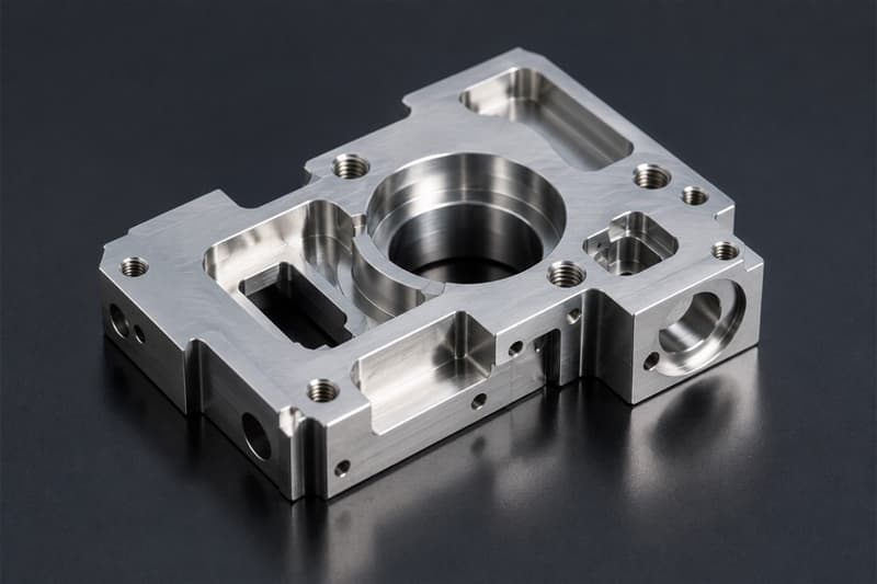
Semiconductor equipment often involves vacuum chambers, gas-control systems, and sealing structures. Traditional die cast parts may contain trapped gas, shrinkage porosity, or micro-voids, especially in thick sections. Even when a part passes visual and dimensional inspection, these internal defects may still cause micro-leakage during vacuum testing.
For this reason, die casting design should evaluate gate location, runner balance, venting, overflow design, wall-thickness transitions, and local hot spots from the beginning. Vacuum-assisted die casting and mold-flow analysis can also be used when appropriate to reduce gas entrapment and internal porosity.
Precision machining is equally important in sealing areas. O-ring grooves, sealing surfaces, and mating faces with excessive tool marks, insufficient flatness, or local distortion may create microscopic leakage paths even when the base material itself is sound.
Vacuum components therefore require control of both internal material quality and the geometry of critical sealing surfaces.
High-End Semiconductor Components Depend on Geometric Relationships, Not Just Dimensions
Semiconductor handling systems, robotic arms, and precision positioning modules require high repeatability and assembly accuracy.
The critical requirement is often not a single hole diameter, but the geometric relationship between holes, datum surfaces, bearing seats, and mounting faces. Flatness, parallelism, perpendicularity, position, and concentricity can be more important than individual dimensional tolerances.
If spindle runout is excessive, fixturing is unstable, or tool wear is not properly controlled, accumulated error can lead to eccentricity, assembly interference, or motion deviation even when each individual dimension remains within tolerance.
High-precision machining therefore requires control of spindle condition, tool compensation, fixture design, machining datums, and measurement strategy—not just final dimensional inspection.
Critical features can be monitored through coordinate measuring machines and statistical process control. Where specific customer requirements apply, appropriate process capability targets and inspection plans can be defined for key dimensions.
Surface Roughness Affects Sealing, Coating Quality, and Cleanliness
Semiconductor components often require anodizing, conversion coating, plating, or other specialized surface treatments. The machined surface condition before finishing can directly influence coating uniformity and adhesion.
Scratches, burrs, micro-cracks, or excessive roughness may become more visible after surface treatment and can also affect sealing performance, cleaning efficiency, and cleanroom assembly.
For vacuum sealing surfaces, thermal contact surfaces, and precision fixtures, surface roughness should be specified according to function rather than simply minimized as much as possible.
An overly rough thermal interface can reduce actual contact area, while inappropriate machining marks on a sealing surface may increase the risk of micro-leakage.
Surface roughness, flatness, machining direction, and final surface treatment should therefore be considered together during the design stage.
Thermal Management and Flatness Are Equally Important
Test fixtures, thermal bases, and high-power semiconductor equipment require both good thermal conductivity and stable contact surfaces.
If contact-surface flatness is insufficient, actual heat-transfer area is reduced and local thermal resistance can increase, resulting in uneven temperature distribution.
In precision testing or measurement equipment, temperature gradients may also cause localized thermal expansion, which can affect dimensions and positioning accuracy.
Thermal components for semiconductor equipment should therefore be evaluated based on material conductivity, machining flatness, surface roughness, heat-source location, and structural rigidity as a complete system.
Tool Wear Directly Affects Production Consistency
Semiconductor equipment components commonly use aluminum alloys, stainless steels, high-silicon aluminum alloys, and engineering plastics. Each material produces different tool-wear behavior.
The hard silicon particles in high-silicon aluminum alloys can accelerate abrasive tool wear. In conventional aluminum machining, inadequate chip evacuation or lubrication can cause built-up edge and adhesive wear. Over time, these conditions can affect bore diameter, surface finish, and geometric accuracy.
For mass production, fixed cutting parameters alone are not sufficient. Tool-life management, tool compensation, and critical-dimension monitoring should be incorporated into the process.
Stable spindle rigidity, appropriate cutting speed and feed rate, effective chip evacuation, and proper cooling can reduce heat buildup and abnormal tool wear while improving batch-to-batch consistency and machining efficiency.